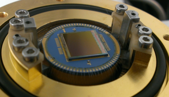
Innovative detectors and focal planes are crucial developments to take the next leap for astronomical observatories. Reducing the read-out noise, increasing the quantum efficiency, enable large format low noise detectors, as well as curved ones, are amongst the main challenging activities. Moreover, shaping the beams before the detector plane is a fundamental step that can benefit from innovative developments on freeform optics and novel optical design methods.
-
Low noise OCAM camera
For the first time, subelectron readout noise has been achieved with a camera dedicated to astronomical wavefront-sensing applications. The OCam system demonstrated this performance at a 1300 Hz frame rate and with 240 × 240 pixel frame size. ESO and JRA2 OPTICON jointly funded e2v Technologies to develop a custom CCD for adaptive optics (AO) wavefront-sensing applications. The device, called CCD220, is a compact Peltier-cooled 240 × 240 240 × 240 pixel frame-transfer eight-output back-illuminated sensor using the EMCCD technology. A second version of OCam, called OCam2, has been designed to offer enhanced performance, a completely sealed camera package, and an additional Peltier stage to facilitate operation on a telescope or environmentally challenging applications. This instrumental development will strongly impact the performance of the most advanced AO systems to come.
-
Low light level CCD : L3CCD science grade detector
The CCD282 is a large low-light level (L3 – Electron multiplying CCD) imaging sensor developed by e2v technologies for the University of Montreal. The intended use is for photon counting and very low light level imaging. The device will be used on the 3DNTT instrument which is a scanning Fabry-Perot interferometer. There is also the intention to place a device on a 10m class telescope for scanning Fabry-Perot application. This sensor is the largest electron multiplying CCD device produced to date with a 4kx4k backside illuminated frame transfer architecture. The sensor uses 8 parallel EM (Electron Multiplying) amplified outputs to maximize throughput. The clock induced charge (CIC) which is one order of magnitude lower than previous devices thanks to a specific design optimized for photon counting operation.
-
Natural Guide Star Detector for adaptive optics : NGSD
The success of the next generation of instruments for ELT class telescopes will depend upon improving the image quality by exploiting sophisticated Adaptive Optics (AO) systems. One of the critical components of the AO systems for the E-ELT has been identified as the optical Laser/Natural Guide Star WFS detector. The combination of large format, 1760×1680 of 24 μm pixels to finely sample the wavefront and the spot elongation of laser guide stars, fast frame rate of 700 frames per second (fps), low read noise (< 3e-), and high QE (>90%) makes the development of this device extremely challenging. Design studies concluded that a highly integrated Backside Illuminated CMOS Imager built on High Resistivity silicon as the most likely technology to succeed. Two generations of the CMOS Imager are being developed : a) the already designed and manufactured NGSD, a quarter sized pioneering device of 880×840 pixels capable of meeting first light needs of the E-ELT ; b) the LGSD, the larger full size device. The detailed design is presented including the approach of using massive parallelism (70,400 ADCs) to achieve the low read noise at high pixel rates of 3 Gpixel/s and the 88 channel, 220 Mbps, LVDS serial interface to get the digitized data off-chip.
-
Spectral-sensitive detectors
Up to now detectors in the visible and infrared are not sensitive to the incident wavelength. To make colored images, multispectral or hyperspectral imaging the solutions were to add filters, this is widely used with the bayer method on commercial imagers, use vertical CMOS structures like the FOVEON X3 sensor or use different materials with different cutoff wavelengths (bispectral sensors used in the inferared for example). The drawback of these methods is that it uses rejection methods to determine the photons wavelengths. Therefore the amount of detection bands is usually fixed to a few, their spatial resolution is degraded accordingly, and the overall sensitivity is decreased. Our development uses a different approach using avalanche photodiodes (APD) and has a high degree of versatility. When a photon is absorbed in the avalanche region of the APD, the gain varies with the absorption depth. As the absorption depths is dependent upon the photon wavelength, such a system coupled with a photon counting amplifier permits to determine the photon wavelength with an amplitude measurement of the output diode. The effect has been demonstrated with single element silicon photodiodes. Patent FR2968836(B1), US2013335742(A1), WO2012080256(A3)
-
Curved and deformable detectors
Up to now detectors have been fabricated with a planar shape, using standard manufacturing processes of the microelectronics industry. But this constrains the forefront optics. Moreover mapping a spherical field of view onto a planar device is very difficult for wide field of views. It is possible to relax the constraints of the imaging optics when using a curved focal plane. The challenge is then to curve the electronic detector to fit within the focal plane shape. This is made possible by thinning the detector and gluing it onto a curved or a variable curvature elastic substrate with the appropriate process. This method has been demonstrated for various visible and infrared devices, including the extremely complex infrared focal plane arrays. The challenge is now to determine precisely the limits of the method and develop an industrial scale process to make these devices widely available. Patent pending. Contacts at CEA-LETI.
-
MOEMS components
MOEMS components have the ability to fully shape the incident light in terms of intensity or object selection with programmable slits, in terms of phase or wavefront control with deformable micromirrors, and finally, in terms of spectrum with programmable diffraction gratings. These three types of components are developed and studied at the LAM for applications in multi-object spectroscopy, in wavefront correction (adaptive optics) and for programmable spectrographs.
The LAM relies on close collaborations with European microtechnology laboratories, in particular with the LAAS in Toulouse, the EPFL in Neuchâtel (Switzerland) and the CSEM (Switzerland), for the design and realization of components.
As an example (Fig. 1), we have developed with EPFL and have been able to operate a first European prototype of steerable micromirrors, MIRA, at cryogenic temperatures of 162K and under vacuum. The interferometric measurement of the mirror surface shows its excellent quality at this temperature and in operation (Fig. 1). The second generation is underway with arrays of up to 20,000 micro-mirrors of 100×200µm2, made of single crystal silicon.
All characterizations are performed at the LAM on benches that we have designed and implemented, including an interferometric bench with sub-nanometric measurement accuracy and an operational characterization bench that can simulate an astronomical observation field.
In 2017, we operated for the first time a deformable MOEMS mirror (US component Iris-AO) at 160K and in vacuum, to be able to control the incident wavefront at the entrance of our future instruments on the ground (infrared instruments) and in space. Using the test facilities described for MIRA, we have developed at LAM the algorithms allowing the component to operate optimally at 293K and 160K: we have reached a best flat of 10nm rms at 293K; at 160K, the mirror deforms by more than 500nm PtV; we bring the best flat back to 12nm rms using our procedure.
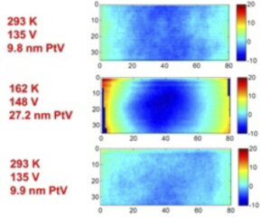
Surface characterization at room temperature (293K) and at 162K of MIRA, European micro-mirror array. 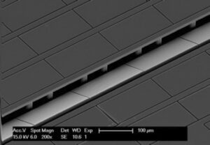
MIRA, European micromirror array (mirrors of 100×200µm2
mirrors made of single crystal silicon), seen with a scanning electron microscope. -
MOEMS-based instrumentation: the BATMAN family
The formation and evolution of galaxies, stellar physics, detection and characterization of solar system objects, all these challenges can be met with a new generation of instruments for astrophysics. In these families of instruments, spectro-imagers play a key role because they allow to access simultaneously to the photometry and the spectroscopy of the observed scenes. We are currently developing such a class of instruments at the LAM, using several breakthrough technologies such as micro-mirror arrays (MMA) for object selection and diffraction gratings on convex substrates. We have nicknamed this new generation of spectro-imagers BATMAN (Fig. 2).
Its demonstrator, ROBIN, has been fully developed and integrated at LAM. It has demonstrated the exceptional capabilities of this instrument. The mounting of our instrument on the Italian Telescopio Nazionale Galileo (TNG) of 3.6m in the Canary Islands will allow remarkable astrophysical discoveries. The spin-offs of this project in the longer term will be on ground-based telescopes (Gemini of 8m diameter, in 2026) or in space.
We have also decided to equip the VLT, the European telescope of 8m diameter in Chile, with a new version of BATMAN, BATMAN@MAVIS, with performances unequalled in the world; it will be placed behind MAVIS, the new multi-conjugate adaptive optics system in the visible.
This work is carried out in the framework of numerous national and international projects with observatories in Italy, Great Britain and Spain, with funding from national research organizations, space agencies (CNES, ESA), Europe, as well as the Provence-Alpes-Côte d’Azur Region (Région SUD) and the Conseil Départemental des Bouches-du-Rhône.
Advances in optics-photonics could have wider repercussions in the field of optical instrumentation for Earth Observation from space, or in the fields of physics and biology.
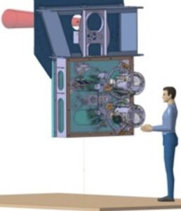
Concept and representation of the BATMAN instrument mounted in the foyer of the TNG. 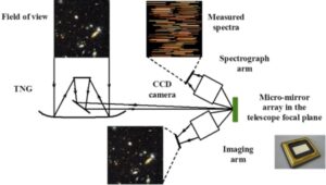
BATMAN, a new generation spectro-imager, based on an array of
mirrors to simultaneously address an imager and a spectrograph.
